by Kristian Vättö on November 7, 2013 9:00 AM EST
The shopping season is getting busier and busier as we get closer to the holidays. This is a season that no manufacturer wants to miss because statistically speaking the holiday season accounts for about one fifth of all the retail sales in the US. It's no coincidence that we also see a ton of product releases before the holiday shopping season or right at the beginning of it. For manufacturers it's crucial to have a competitive and up-to-date lineup because no company wants to miss the chance of generating potentially over 20% of their annual revenue.
The SSD market is no exception to the rule. While an SSD may not be the first gift idea to come to your mind, the shipments increase temporarily in Q4 where the holiday shopping season falls. There's even some actual data from a research firm IHS.
| Worldwide SSD Shipments | |||||
| Q1'12 | Q2'12 | Q3'12 | Q4'12 | Q1'13 | |
| Units (in Millions) | 6.0 | 7.3 | 9.3 | 12.1 | 11.5 |
Part of the reason for the increase is of course the increased sales of PCs, of which some come with a pre-installed SSD. However, the increase is not limited to PC sales as the holiday season is also a busy time for new builds and upgrading existing computers, both of which impact the retail SSD market.
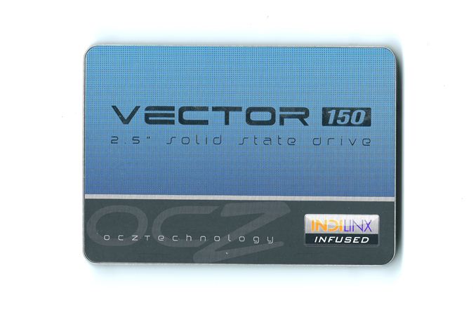
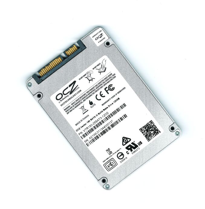
OCZ's answer to the holiday demand is the Vector 150. Like the original Vector and Vertex 450, the Vector 150 is based on OCZ's first fully in-house designed Barefoot 3 controller. OCZ hasn't given out much specifics about the controller other than it's an 8-channel design with two cores (one unnamed ARM Cortex core and OCZ Aragon co-processor). The only change in hardware this round is the switch from 25nm IMFT MLC NAND to Toshiba's 19nm MLC NAND. Toshiba announced the production of second generation 19nm NAND in May but the Vector 150 is using the first generation 19nm NAND. I will however save the details of the differences between Toshiba's first and second generation NAND for a review where we have a drive with the second generation NAND.
The change in NAND makes perfect sense because 25nm NAND hasn't been cost effective for a long time and the 19nm/20nm processes have matured enough to meet the criteria for a high-end SSDs. I believe OCZ went with Toshiba's NAND for performance reasons because generally Toshiba's NAND has been a bit faster than IMFT's. Back when OCZ released the Vertex 450, I asked them why didn't they just release an updated Vector with 20nm IMFT NAND. OCZ told me that the 20nm NAND didn't meet their performance standards for a high-end SSD and hence they released the mainstream orientated Vertex 450 and kept using IMFT's 25nm NAND in the Vector. (In case you didn't already know, Vector is OCZ's enthusiast orientated brand, whereas the Vertex is more mainstream focused.) I put down a quick table comparing the differences between the three Barefoot 3 based SSDs that OCZ has in their product portfolio.
| Comparison of OCZ's Barefoot 3 Based SSDs | |||
| Vector 150 | Vector | Vertex 450 | |
| Controller | Indilinx Barefoot 3 | ||
| NAND | 19nm Toshiba | 25nm IMFT | 20nm IMFT |
| Encryption | AES-256 | N/A | AES-256 |
| Endurance | 50GB/day for 5 years | 20GB/day for 5 years | 20GB/day for 3 years |
| Warranty | 5 years | 5 years | 3 years |
There are obviously some performance differences too but since those vary depending on the capacity, I decided to leave them out to keep the table readable. The Vector 150 has two major upgrades over the original Vector: Hardware encryption support and higher endurance. Unlike the original Vector, the Vector 150 (as well as the Vertex 450) supports AES-256 hardware encryption. Unfortunately OCZ's implementation does not support TCG Opal 2.0 and IEEE-1667 specs, so it's not compatible with Windows 8's hardware accelerated BitLocker. The lack of TCG Opal 2.0 support also means that there is no support for encryption software such as Wave and WinMagic, which support hardware accelerated encryption similar to Windows 8's BitLocker. I think more manufacturers should implement these specifications as it makes encrypting a drive much easier with no impact on performance that comes from software implemented encryption. Encryption via ATA password is way more complicated for the end-user and it's also more vulnerable.
The 2.5x increase in endurance is pretty impressive especially when taking into account that we're dealing with smaller lithography NAND with lower endurance. OCZ has achieved the higher endurance with a combination of three things: Advanced flash management and more validation and over-provisioning. OCZ didn't want to go into details about their flash management technologies, which isn't surprising as those technologies tend to be proprietary. However, I would expect at least some sort of adaptive DSP to extend the life of the NAND. Increasing the amount of over-provisioning will lower the write amplification, which in turn will reduce NAND writes and allow for more host writes. As you can see in the table below, OCZ has switched to ~12% stock over-provisioning similar to Corsair's Neutron and SandForce drives.
The final part in the endurance equation is validation. In a perfect world you would just multiply the NAND's P/E cycles with the NAND's capacity to get endurance but unfortunately it's not that simple. You do get the NAND endurance with that equation but there are other parts that need to be taken into account. Validation has to take all potential causes of failure (such as voltage regulators) into account, so the endurance number is a result of the manufacturer's internal validation process. It's an expensive and time consuming process because what you are basically doing is taking hundreds or even thousands of drives and testing them in various environments by writing to them until they die.
It's good to keep in mind that the endurance rating is usually based on a 4KB random write workload, so your NAND writes may end up being way more than 50GB a day. One of the biggest reasons why manufacturers have to limit the warranty with an endurance rating is because otherwise enterprises could use much cheaper consumer SSDs and use the warranty as a basis of getting the drive replaced once they've worn it out. The manufacturers want the enterprise customers to pay the premium for their enterprise SSDs since they've invested on the extra validation required by the enterprise market and it's a market that tends to have higher profits as well.
I do have some unfortunate news when it comes to reliability, though. The 240GB sample OCZ sent us died during our testing. This isn't the first (and I doubt it will be the last) SSD to unexpectedly die during our tests but a failure always raises concern about overall reliability. The drive still drew power (I checked with a multimeter) but it wouldn't show up in the BIOS or Windows. To me this sounds like the inherent power loss issue that nearly all SSDs have.
The problem with SSDs is that once the you lose power, everything in the DRAM cache will be lost. Fortunately manufacturers don't usually store any user data in the DRAM but what they do store is the NAND mapping table for faster access. The NAND mapping table is of course stored in the NAND too but in case there has been changes to the mapping table before the controller has had time to back it up to the NAND, it may corrupt the whole table. A corrupted mapping table means that the controller can't match LBAs to physical NAND locations, so the controller has no idea where your data is. The way SSDs handle this is to go into debug mode, which for some means they won't be recognizable at all or for others they show up as very small volumes (remember the Intel SSD 320 8MB bug?). We don't know yet if this is really the cause of the failure but I did send the drive back to OCZ for failure analysis already and I'll be updating the article as soon as I hear back from them.
| OCZ Vector 150 Specifications | |||
| 120GB | 240GB | 480GB | |
| Controller | Indilinx Barefoot 3 | ||
| NAND | 19nm Toshiba MLC | ||
| DRAM Cache | 512MB | 512MB | 1GB |
| Sequential Read | 550MB/s | 550MB/s | 550MB/s |
| Sequential Write | 450MB/s | 530MB/s | 530MB/s |
| 4KB Random Read | 80K IOPS | 90K IOPS | 100K IOPS |
| 4KB Random Write | 95K IOPS | 95K IOPS | 95K IOPS |
| Steady-state 4KB Random Write | 12K IOPS | 21K IOPS | 26K IOPS |
| Power Consumption | 0.55W Idle / 2.5W Active | ||
| Warranty | 5 years or 91TB of writes | ||
The Vector 150 doesn't support Windows 8's DevSleep functionality, hence the idle power consumption is fairly high. In my opinion it's a bit of let down because most of the high-end SSDs are able to get into very low power states while idle, which results in longer battery life for portable computers. For comparison Samsung's SSD 840 Pro draws only 36.6 milliwatts while idle with HIPM and DIPM enabled, so the difference is over tenfold.
It's also good to see OCZ reporting steady-state random write numbers. The peak numbers are only meaningful if you're dealing with an empty drive and hence it's good that manufacturers are being more open about the performance when dealing with a heavily used drive. I hope more manufacturers will follow suit and start including steady-state numbers as a part of the product specifcations.
As I described above, the 5-year warranty has an endurance condition. The warranty is 5 years or 91TB of writes, whatever comes first. The 91TB figure is derived from 50GB of writes per day (50GB x 365 x 5) and it's the same for all capacities. OCZ did tell me that they're willing to look into individual cases in case the drive dies after 95TB of writes for example but users who will be writing more than 50GB a day should still look into enterprise solutions.
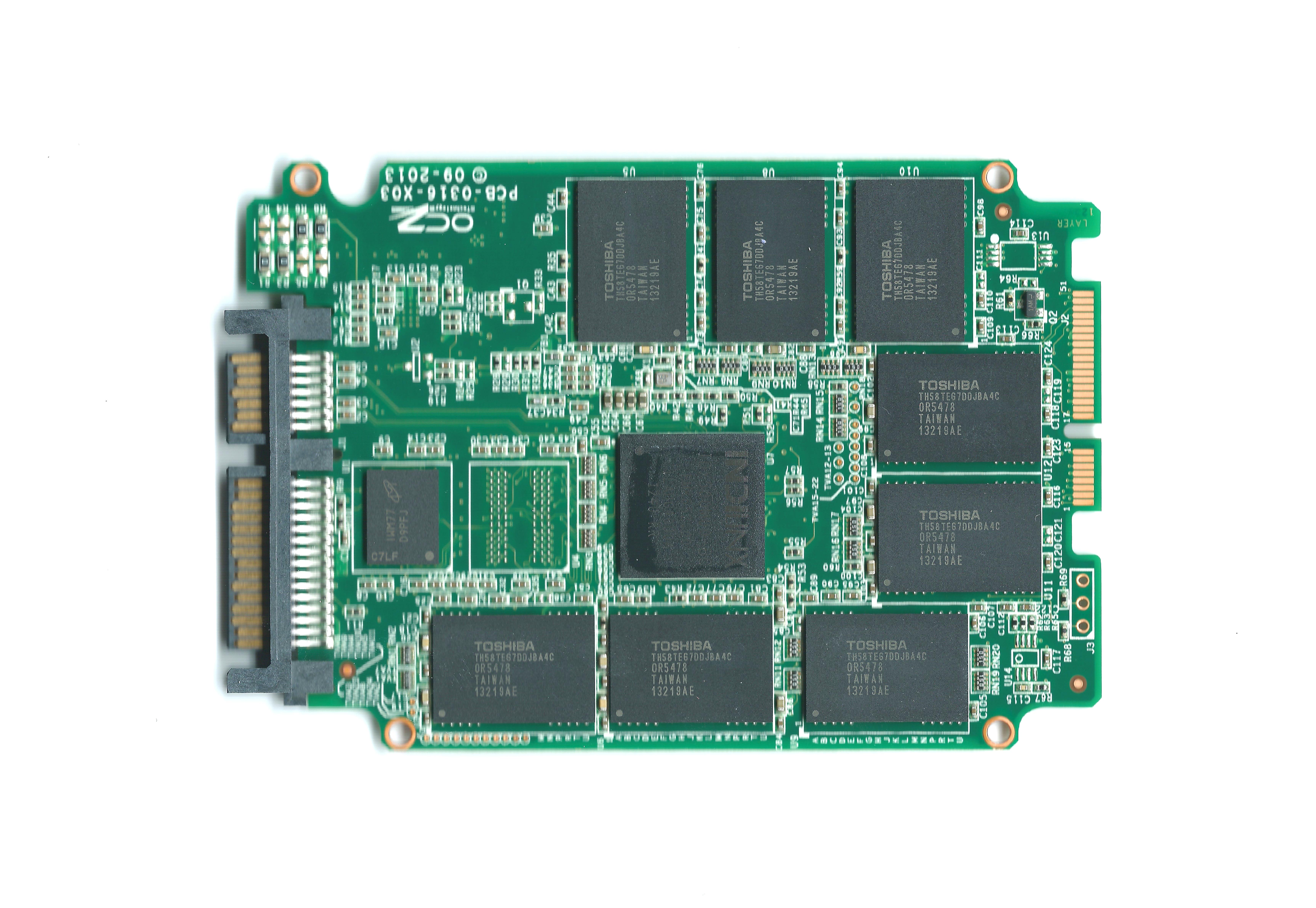
With the original Vector OCZ bought NAND in wafers from Micron and did their own validation and packaging. With the Vector 150 (and Vertex 450) that has changed and OCZ uses pre-packaged NAND from Toshiba. I believe NAND OEMs aren't very willing to sell their latest generation NAND in wafers because they know the profit margins are much better with pre-packaged NAND and with limited supply the clients don't have very many options. There's a total of 16 NAND packages (2x8GB each), eight on each side of the PCB. There are also two Micron 256MB DDR3-1600 chips working as a cache.
Test System
| CPU | Intel Core i5-2500K running at 3.3GHz (Turbo and EIST enabled) |
| Motherboard | AsRock Z68 Pro3 |
| Chipset | Intel Z68 |
| Chipset Drivers | Intel 9.1.1.1015 + Intel RST 10.2 |
| Memory | G.Skill RipjawsX DDR3-1600 4 x 8GB (9-9-9-24) |
| Video Card | XFX AMD Radeon HD 6850 XXX (800MHz core clock; 4.2GHz GDDR5 effective) |
| Video Drivers | AMD Catalyst 10.1 |
| Desktop Resolution | 1920 x 1080 |
| OS | Windows 7 x64 |
Thanks to G.Skill for the RipjawsX 32GB DDR3 DRAM kit
Source:AnandTech.
AnandTech Storage Bench 2013-Here-
Source:AnandTech.
AnandTech Storage Bench 2013-Here-